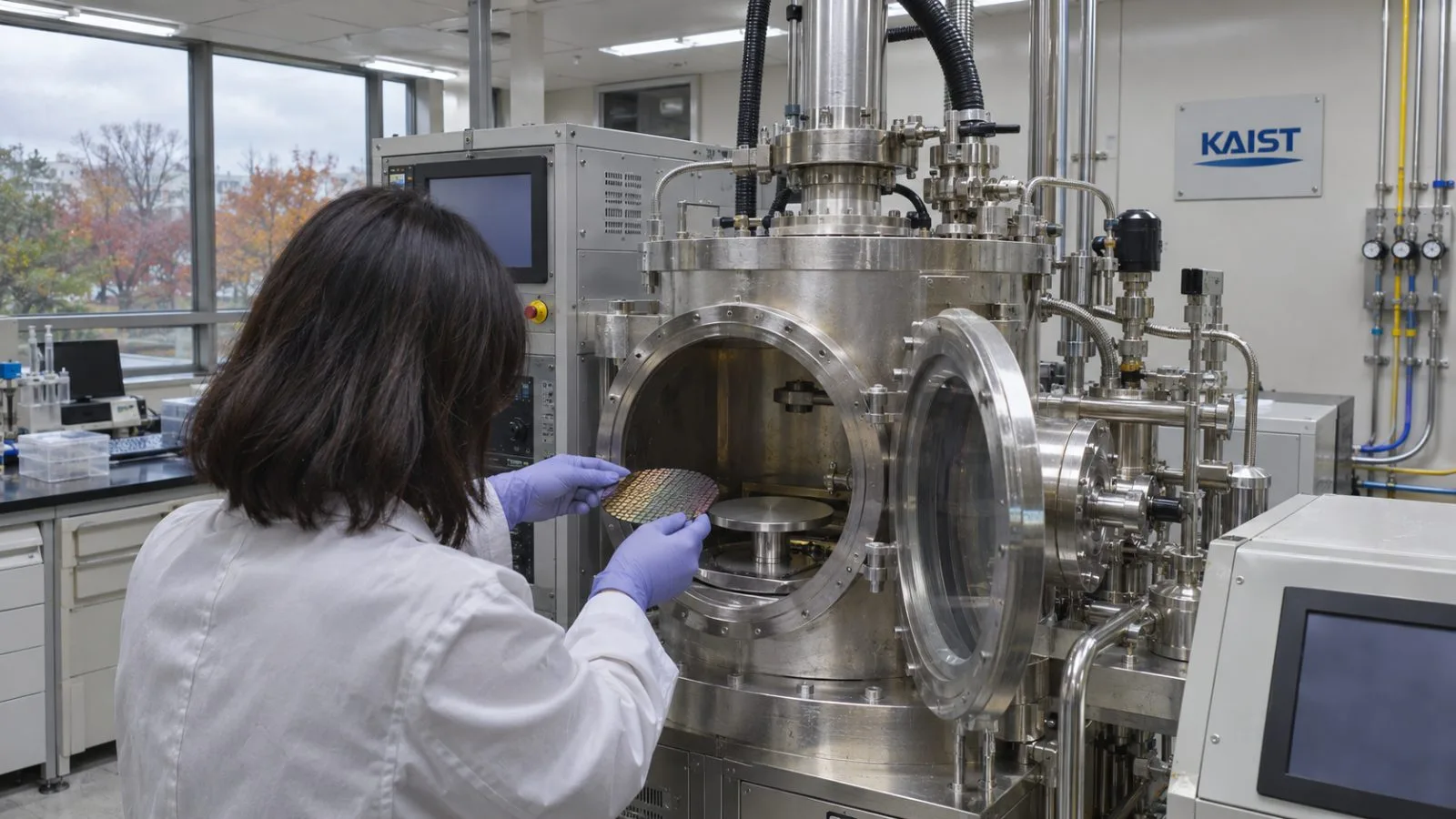
A KAIST-led research team reported a method for controlling where molybdenum disulfide crystals start growing, with single crystals forming at more than 99% of 400 patterned sites. The result could help researchers place two-dimensional semiconductors more precisely on chips, a possible use KAIST identified for the approach. Researchers from Hanyang University and UNIST collaborated, and the study appeared online in Nature on Oct. 7.
The team calls the process etching-flux-mediated single-centred nucleation (EF-SCN). It uses oxygen released by an oxide barrier to suppress new crystal formation near the edges of each patterned area. This leaves a nucleus near the center to expand into a single crystal. Hanyang University said the hafnium oxide barrier released oxygen when heated to 750°C. The researchers deposited MoS₂ using metal-organic chemical vapor deposition.
KAIST said the method produced a central single crystal at more than 99% of the 400 sites. Hanyang University said the test covered a two-centimeter substrate. The paper reports field-effect mobility of up to 117 cm² V⁻¹ s⁻¹. Hanyang said the researchers placed four transistors in one crystal, with electron mobility varying by 7.8%. Replacing hafnium oxide with zirconium dioxide allowed growth at temperatures as low as 430°C, according to the paper.
The study focuses on nucleation, the first point at which a crystal begins to form. The paper contrasts the method with area-selective approaches, which can confine growth to chosen regions while leaving the exact starting point within each region uncertain. KAIST said crystals that begin at multiple spots can meet at grain boundaries that hinder electron movement. KAIST Professor Kibum Kang described the location where a crystal forms as “inherently a matter of probability.” The team’s approach aims to steer crystal formation toward the center.
The reported results concern MoS₂. KAIST identified direct growth of two-dimensional semiconductors on chips as a possible future application.