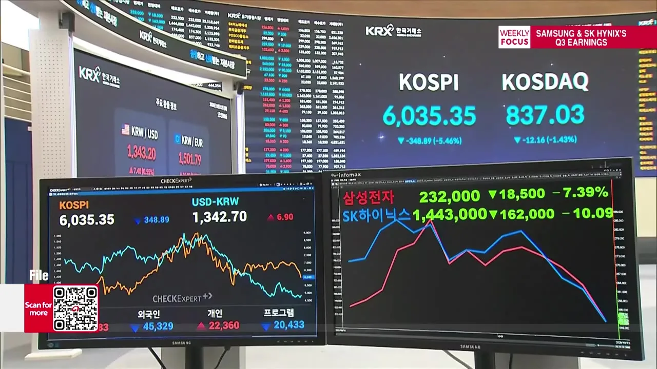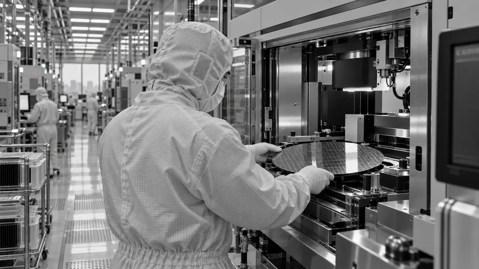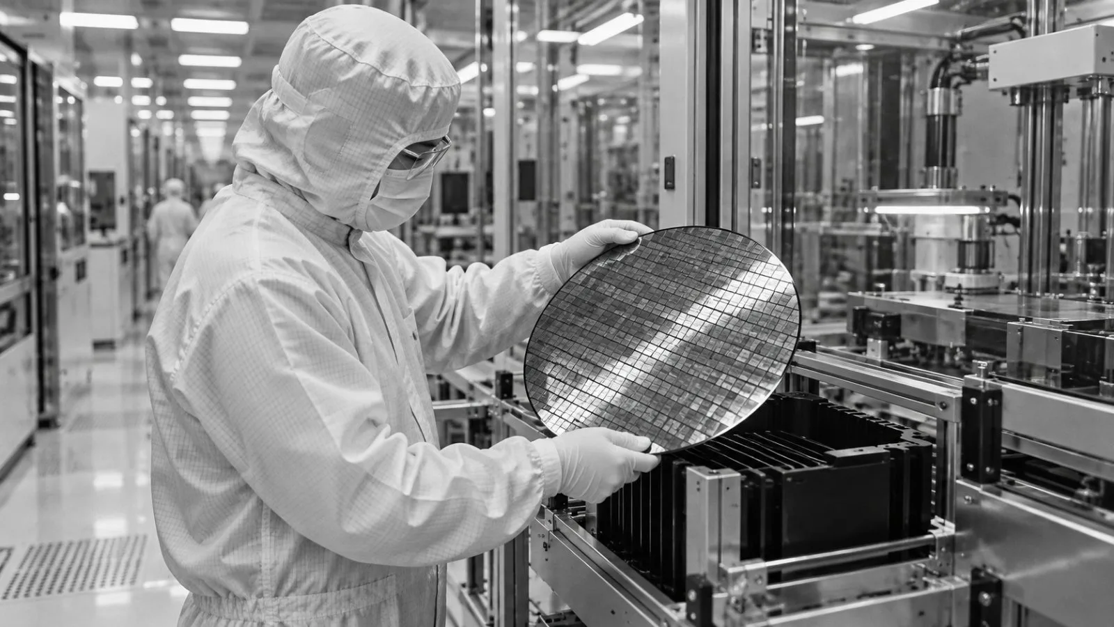
Samsung Electronics aims to develop its Yokohama research site into an international center for advanced chip packaging, a field tied to competition in AI semiconductors, The Korea Herald reported Sunday.
Executive Chair Lee Jae-yong visited the Advanced Package Lab (APL) on Sunday. The newspaper reported that he reviewed research on packaging materials and manufacturing processes with researchers at the facility. It also said Lee stressed the need for advanced packaging technology to strengthen Samsung’s position in AI chips.
Samsung said Lee discussed cooperation with Japanese suppliers of semiconductor materials, components and equipment, according to the report. The Korea Herald said Samsung wants APL to research next-generation packaging approaches, including advanced bonding and glass substrates.
The Korea Herald reported that APL is expected to coordinate with Samsung’s semiconductor research teams in South Korea. The newspaper described the Yokohama facility as a way to draw on Samsung’s chip design and manufacturing capabilities alongside Japan’s semiconductor supplier base.