SpaceX Pushes for Early Stock Index Inclusion Ahead of Potential Record-Breaking IPO
  Sam Altman Reaffirms OpenAI’s Long-Term Commitment to NVIDIA Amid Chip Report
  CK Hutchison Launches Arbitration After Panama Court Revokes Canal Port Licences
  Sony Q3 Profit Jumps on Gaming and Image Sensors, Full-Year Outlook Raised
  TSMC Eyes 3nm Chip Production in Japan with $17 Billion Kumamoto Investment
  Nvidia CEO Jensen Huang Says AI Investment Boom Is Just Beginning as NVDA Shares Surge
  SpaceX Prioritizes Moon Mission Before Mars as Starship Development Accelerates
  SoftBank and Intel Partner to Develop Next-Generation Memory Chips for AI Data Centers
  Nvidia, ByteDance, and the U.S.-China AI Chip Standoff Over H200 Exports
  FDA Targets Hims & Hers Over $49 Weight-Loss Pill, Raising Legal and Safety Concerns
  Tencent Shares Slide After WeChat Restricts YuanBao AI Promotional Links
  Google Cloud and Liberty Global Forge Strategic AI Partnership to Transform European Telecom Services
  AMD Shares Slide Despite Earnings Beat as Cautious Revenue Outlook Weighs on Stock
  Indian Refiners Scale Back Russian Oil Imports as U.S.-India Trade Deal Advances
  Uber Ordered to Pay $8.5 Million in Bellwether Sexual Assault Lawsuit


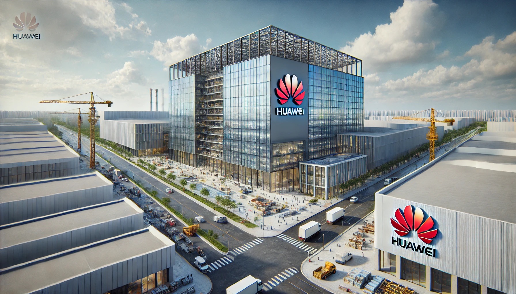
Huawei is set to complete its new research and development facility in Guangzhou by September, which will house 5,000 employees.
As a result of the trade penalties imposed by the United States, Huawei and other Chinese businesses are unable to purchase cutting-edge chipmaking equipment from ASML, which is situated in the Netherlands. Furthermore, there is no possibility that they will be able to acquire cutting-edge wafers from TSMC.
While it appears that Huawei's relationship with SMIC, the largest semiconductor manufacturer in China, is proceeding without a hitch, it is quite likely that Huawei wants chip development to be accelerated to an extreme degree.
Huge Sums Invested in New R&D Center
This is the reason why it was earlier claimed that huge sums of money had been invested in a brand new research and development center that would be situated in Guangzhou and would serve this purpose.
Currently, the first photographs that are considered to be "official" have been released, which depict what the facility would look like both inside and outside. It is possible that this initiative may become the foundation upon which Huawei will build its ability to manufacture wafers of the next generation, but only time will tell at this point.
According to a report by CnBeta, which discovered photographs of Huawei's research and development facility through a WeChat account titled China Guangzhou Release, the Phase I center that is situated in the New Coast region of the Bay Area is anticipated to be finished in September of this year.
The fact that the term "Phase I" is included gives the impression that this is not the only facility that Huawei is aiming to construct. However, it also gives the impression that the erstwhile Chinese behemoth is planning something of enormous dimensions.
Per WCCFTECH, the study indicates that the project encompasses around 119,300 square meters of land, with a total construction area of roughly 305,000 square meters. This information pertains to the region.
Facility to House 5,000 Employees
A total of eight research and development buildings, one hotel, one cooling tower, a guard room, and two basements are included in Phase I. The entire building is expected to be able to house 5,000 workers for research and development as well as office use once it is finished in September.
The research and development facility of Huawei, on the other hand, is believed to occupy an area equivalent to 224 football fields and is anticipated to house 35,000 personnel, according to an earlier report.
It would appear that additional work is required, the completion of which might result in a period of several years.
Phase I to Focus on Cloud Computing and IoT
According to a number of publications, Phase I will be responsible for doing research and development in the areas of cloud computing, Internet of Things, and smart cars; however, it does not include the production of chips under any circumstances. In light of the fact that Huawei was reported to have spent approximately ¥12 billion, which is equivalent to $1.66 billion, on the facility, we anticipate that other surprises will be forthcoming in the future.
For the time being, Huawei may have little choice but to rely on SMIC. Considering that SMIC was previously believed to have successfully developed its 5nm process, it is likely that it will take some time for the Chinese company to have its own sophisticated chipmaking plant up and running.