Samsung Electronics’ planned second foundry in Taylor, Texas, has reportedly secured buyers for its full planned output of HBM base dies, giving the plant customers ahead of its 2030 production target.
Maeil Business Newspaper reported Nov. 3, citing industry sources, that purchase commitments from Advanced Micro Devices (AMD) and Nvidia together match the amount of base-die production planned for the facility. AMD was reported to have the larger share.
Samsung has not publicly named customers for Fab 2. A company representative told Maeil that customer-related matters were difficult to confirm.
At a July 30 earnings call, Sukchae Kang, Samsung Electronics executive vice president and head of sales and marketing for Foundry, said construction was planned to begin by year-end, with “mass production by 2030” as the target. Samsung linked the schedule to customer demand exceeding advanced-node capacity, but did not name specific customers on the call.
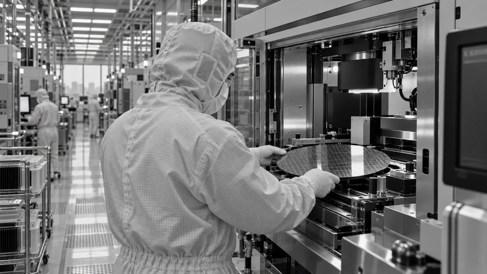
Maeil said the plant is planned to use a 2-nanometer process and cover about 2.7 million square feet (250,000 square meters), roughly 1.5 times the size of Samsung’s first Taylor facility. Samsung’s 2025 public disclosure separately listed a semiconductor contract with Tesla worth 22.76 trillion won (about $16.54 billion), running through Dec. 31, 2033. The filing did not identify the plant; Maeil described Tesla work at the first Taylor fab.
HBM packages stack DRAM chips, with a base die providing the logic layer that links the memory stack to a graphics processing unit (GPU). Maeil also reported that Nvidia is seeking to have Taiwan Semiconductor Manufacturing Co. (TSMC) produce base dies for its custom NVHBM standard. It did not identify which Nvidia products or memory variants might use dies planned for Taylor.
Maeil reported that site preparation had begun, formal construction was expected in November 2026 and equipment installation was scheduled to start in February 2029. Samsung’s stated mass-production target is 2030.