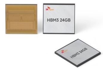
SK hynix has developed the first 12-layer stacked high bandwidth memory (HBM3) chip, which vertically interconnects multiple DRAM chips to increase data processing speed.s.
The 24GB package product increased memory capacity by 50 percent from the previous product
SK hynix, which developed the first-generation HBM in 2013, said it expects the product to be in high demand in sectors such as artificial intelligence (AI) that require a high capacity and fast data processing.
It is currently validating its performance with customers and will be able to start supplying the new products in the second half of the year/
HBM3 succeeds the previous generations of HBM, HBM2, and HBM2E.
According to SK hynix, it was able to develop the 12-layer product because its engineers improved process efficiency and performance stability by applying advanced mass reflow molded underfill technology.
The company also applied through-silicon via (TSV) technology to reduce the thickness of a single DRAM chip by 40 percent and achieved the same stack height level as the 16-gigabyte product.