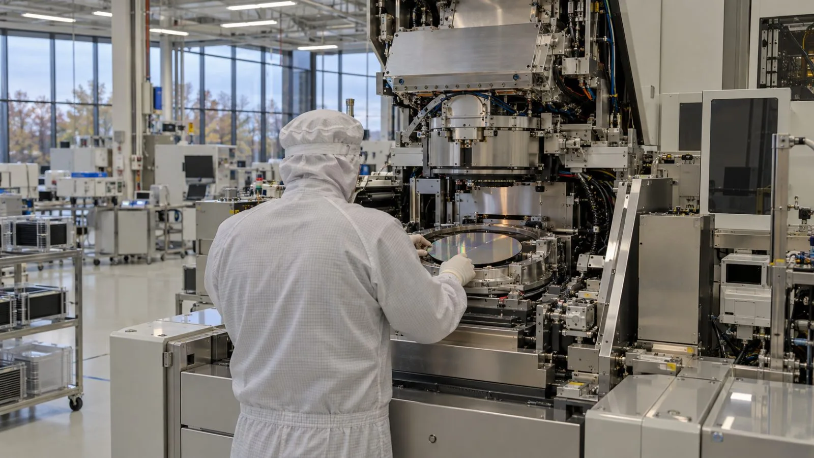
JNTC has moved its through-glass-via (TGV) substrates into paid sampling with NVIDIA, a commercial step that is not a production order and comes ahead of a mid-2028 supply target.
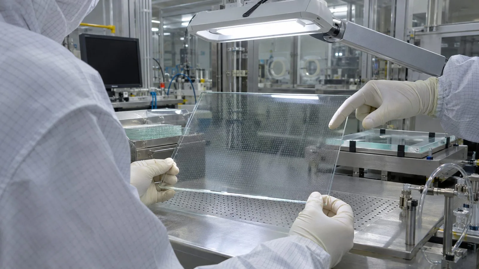
A 2 mm-thick TGV glass substrate JNTC developed in June recorded peel strength of about 0.8 kilogram-force per millimeter (kgf/mm), double the stated industry benchmark of 0.4 kgf/mm. Testing found no microcracks after copper was removed.
JNTC's method combines glass drilling with etching, metal deposition and chemical mechanical polishing. Weak bonding can crack glass beside a via or split it when a built-up substrate is cut into individual pieces. Glass is under consideration for advanced packaging as AI chips grow larger and more complex.
NVIDIA's procurement roster included JNTC roughly a month after the South Korean company first approached the chipmaker in September 2026. The status permits paid purchases after initial quality screening but does not indicate a mass-production commitment.
Customers first receive a small number of free units for specification changes and basic reliability testing. Later paid batches may number in the hundreds or thousands, helping buyers judge whether quality and yield can hold at production scale. Substrate manufacturers or outsourced semiconductor assembly and test (OSAT) providers may add build-up layers, assemble chips and evaluate reliability.
For Broadcom, JNTC is also working with Japan's Toppan on TGV substrates. JNTC has nondisclosure agreements with roughly 30 substrate manufacturers, chip companies and OSAT providers; about 10 counterparties are reviewing paid samples.
JNTC expects its Hwaseong pilot line to support customer samples. Construction work on the Gimcheon production line is planned for the second half of 2027, and JNTC's target for initial production supply is mid-2028.