


 Kingboard Holdings Shares Surge After HK$11.77 Billion Block Trade to Expand PCB and AI Supply Chain Business
  Frank Stronach Found Guilty of Sexual Assault and Indecent Assault in Ontario Court
  Qantas Unveils Wellness-Focused Nonstop Sydney-London Flights to Reduce Jet Lag
  Jio IPO Filing Nears as Reliance Targets $4 Billion Market Debut
  BHP Shares Fall as Jansen Potash Project Costs Surge
  Meta Seeks Legal Shield From Child-Harm Lawsuits Amid KOSA Talks
  Trump Says Anthropic No Longer Seen as National Security Threat
  Hanmi Semicon Shares Surge After $33 Million SpaceX Investment
  Trump Administration Delays DeepSeek and CXMT Trade Blacklist Designations Amid U.S.-China Tensions
  GM and Lockheed Martin Partner to Strengthen U.S. Defense Manufacturing Capacity
  US Raises Concerns Over Possible ASML EUV Machine Transfer to China
  SpaceX IPO Set for Explosive Debut as Valuation Tops $2.2 Trillion
  UK Banks Report Surge in APP Fraud Losses as Pressure Mounts on Meta and Tech Platforms
  Google Gemini Co-Lead Noam Shazeer Leaves for OpenAI Amid AI Talent Race
  Anthropic Restricts Global Access to AI Models After U.S. Security Review
  SpaceX IPO Sparks Market Optimism as Shares Surge 19% on Trading Debut
  Meta AI Strategy Faces Challenges as Zuckerberg Admits Mistakes in Internal Memo


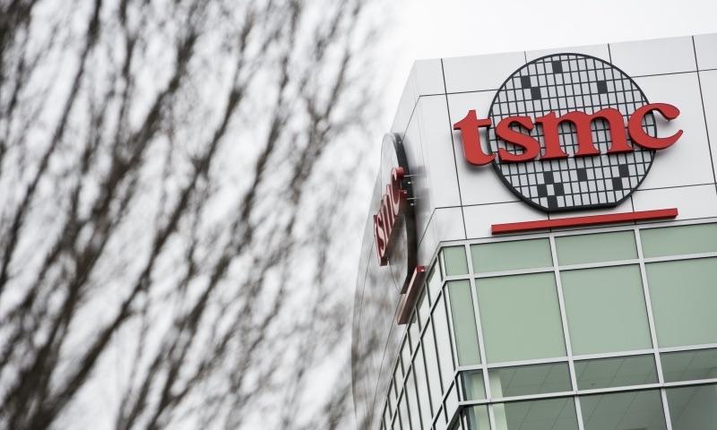
Taiwan Semiconductor Manufacturing Co. (TSMC), the world’s leading contract chipmaker, is nearing completion of a cutting-edge chip packaging technology to meet surging demand for high-performance AI chips, according to Nikkei Asia.
TSMC is developing a square substrate packaging method, diverging from the current industry standard of round substrates. This new approach will allow more semiconductors to be integrated within a single chip, significantly boosting computing power — a critical need for generative AI applications. Small-scale production is expected to begin by 2027, with a dedicated production line under construction in Taoyuan, Taiwan.
Chip packaging is one of the final and most vital steps in semiconductor production. It involves encasing chips in a substrate to connect them into broader electronic systems. TSMC’s new packaging technique expands on its existing CoWoS (Chip-on-Wafer-on-Substrate) technology, which has already proven instrumental in AI chip development.
Major tech giants including Nvidia, AMD, Google, Amazon, and Broadcom rely on TSMC’s CoWoS solutions to power their AI hardware. As demand for generative AI continues to rise, so does the need for enhanced chip performance, making packaging innovations essential.
Over the past two years, TSMC has seen strong growth fueled by the AI boom and increasing global semiconductor demand. With its latest packaging innovation, TSMC aims to solidify its dominance in the AI chip manufacturing space and remain a pivotal force in the global semiconductor supply chain.


