
Semiconductors are a critical part of almost every modern electronic device, and the vast majority of semiconductors are made in Tawain. Increasing concerns over the reliance on Taiwain for semiconductors – especially given the tenuous relationship between Taiwan and China – led the U.S. Congress to pass the CHIPS and Science act in late July 2022. The act provides more than US$50 billion in subsidies to boost U.S. semiconductor production and has been widely covered in the news. Trevor Thornton, an electrical engineer who studies semiconductors, explains what these devices are and how they are made.

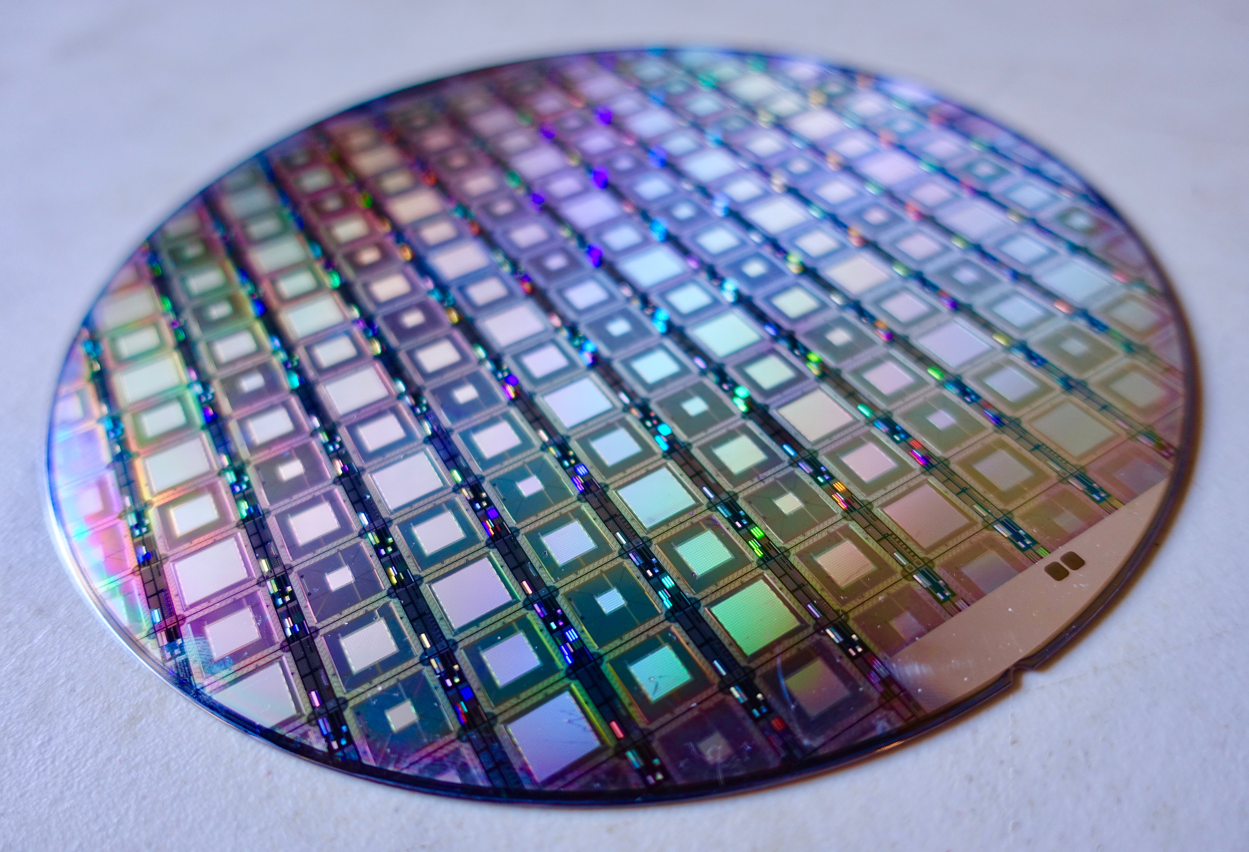
Thin, round slices of silicon crystals, called wafers, are the starting point for most semiconductor chips. Hebbe/Wikimedia Commons
1. What is a semiconductor?
Generally speaking, the term semiconductor refers to a material – like silicon – that can conduct electricity much better than an insulator such as glass, but not as well as metals like copper or aluminum. But when people are talking about semiconductors today, they are usually referring to semiconductor chips.
These chips are typically made from thin slices of silicon with complex components laid out on them in specific patterns. These patterns control the flow of current using electrical switches – called transistors – in much the same way you control the electrical current in your home by flipping a switch to turn on a light.
The difference between your house and a semiconductor chip is that semiconductor switches are entirely electrical – no mechanical components to flip – and the chips contain tens of billions of switches in an area not much larger than the size of a fingernail.
2. What do semiconductors do?
Semiconductors are how electronic devices process, store and receive information. For instance, memory chips store data and software as binary code, digital chips manipulate the data based on the software instructions, and wireless chips receive data from high-frequency radio transmitters and convert them into electrical signals. These different chips work together under the control of software. Different software applications perform very different tasks, but they all work by switching the transistors that control the current.
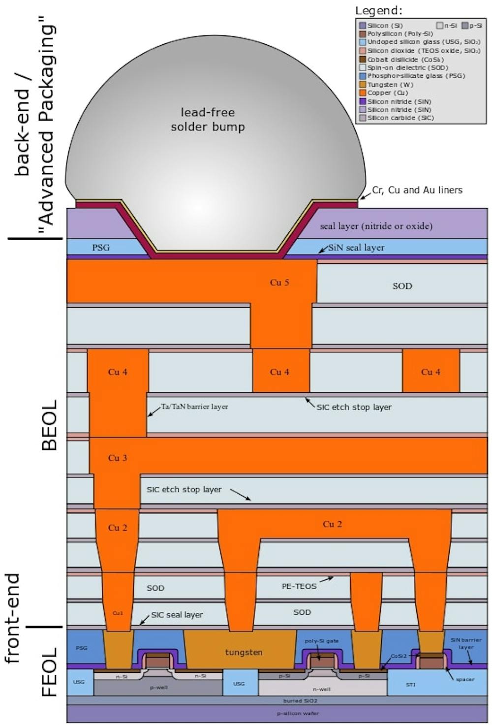
This schematic of a semiconductor chip shows many different materials in different colors and the complicated layering involved in producing a modern chip. Cepheiden/Wikimedia Commons, CC BY
3. How do you build a semiconductor chip?
The starting point for the vast majority of semiconductors is a thin slice of silicon called a wafer. Today’s wafers are the size of dinner plates and are cut from single silicon crystals. Manufacturers add elements like phosphorus and boron in a thin layer at the surface of the silicon to increase the chip’s conductivity. It is in this surface layer where the transistor switches are made.
The transistors are built by adding thin layers of conductive metals, insulators and more silicon to the entire wafer, sketching out patterns on these layers using a complicated process called lithography and then selectively removing these layers using computer-controlled plasmas of highly reactive gases to leave specific patterns and structures. Because the transistors are so small, it is much easier to add materials in layers and then carefully remove unwanted material than it is to place microscopically thin lines of metal or insulators directly onto the chip. By depositing, patterning and etching layers of different materials dozens of times, semiconductor manufacturers can create chips with tens of billions of transistors per square inch.
4. How are chips today different from the early chips?
There are many differences, but the most important is probably the increase in the number of transistors per chip.
Among the earliest commercial applications for semiconductor chips were pocket calculators, which became widely available in the 1970s. These early chips contained a few thousand transistors. In 1989 Intel introduced the the first semiconductors to exceed a million transistors on a single chip. Today, the largest chips contain more than 50 billion transistors. This trend is described by what is known as Moore’s law, which says that the number of transistors on a chip will double approximately every 18 months.
Moore’s law has held up for five decades. But in recent years, the semiconductor industry has had to overcome major challenges – mainly, how to continue shrinking the size of transistors – to continue this pace of advancement.
One solution was to switch from flat, two-dimensional layers to three-dimensional layering with fin-shaped ridges of silicon projecting up above the surface. These 3D chips significantly increased the number of transistors on a chip and are now in widespread use, but they’re also much more difficult to manfacture.
5. Do more complicated chips require more sophisticated factories?
Simply put, yes, the more complicated the chip, the more complicated – and more costly – the factory.
There was a time when almost every U.S. semiconductor company built and maintained its own factories. But today, a new foundry can cost more than $10 billion to build. Only the largest companies can afford that kind of investment. Instead, the majority of semiconductor companies send their designs to independent foundries for manufacturing. Taiwan Semiconductor Manufacturing Co. and GlobalFoundries, headquartered in New York, are two examples of multinational foundries that build chips for other companies. They have the expertise and economies of scale to invest in the hugely expensive technology required to produce next-generation semiconductors.
Ironically, while the transistor and semiconductor chip were invented in the U.S., no state-of-the-art semiconductor foundries are currently on American soil. The U.S. has been here before in the 1980s when there were concerns that Japan would dominate the global memory business. But with the newly passed CHIPS act, Congress has provided the incentives and opportunities for next-generation semiconductors to be manufactured in the U.S.
Perhaps the chips in your next iPhone will be “designed by Apple in California, built in the USA.”
 Trevor Thornton does not work for, consult, own shares in or receive funding from any company or organization that would benefit from this article, and has disclosed no relevant affiliations beyond their academic appointment.



.svg#/media/File:Cmos-chip_structure_in_2000s_(en).svg)