


 Standard Chartered Beats Profit Forecasts as First-Half Earnings Rise 9%
  Tech Stock Positioning Nears Neutral as Investor Rotation Enters Final Phase, Deutsche Bank Says
  Meta CEO Zuckerberg Opposes U.S. Ban on Chinese AI Models, Warns Against Overregulation
  Serica Energy to Acquire Pharos Energy for £145.7M, Sending PHARP Shares Soaring
  TSMC Gradually Restarts Japan Chip Plant After Kumamoto Earthquake
  Brown-Forman Rejects Sazerac’s $15 Billion Takeover Bid as Family Backs Independence
  BHP, Port Hedland Unions Fail to Reach Wage Deal as Negotiations Continue
  Seagate Stock Jumps as AI-Fueled Earnings Beat and Strong FY2027 Outlook Impress Investors
  Zabka Shares Drop 10% as Seven & i Abandons Investment Plans
  Philips Shares Slide 10% Despite Earnings Beat as Weak Orders Raise Growth Concerns
  TeamViewer Shares Fall Despite Profit Growth as ARR and Customer Base Decline
  CATL Shares Jump as $5.6 Billion Buyback Signals Confidence in Long-Term Growth
  AstraZeneca Q2 Earnings Beat Forecasts as Oncology Growth Supports 2026 Outlook
  Exosens H1 Profit Beats Forecasts as Defense Demand Drives Growth
  GSK Unveils $2.52 Billion Cost-Cutting Plan to Accelerate Drug Pipeline
  Air Liquide Q2 Sales Growth Tops Forecast as Electronics Business Drives Strong Performance


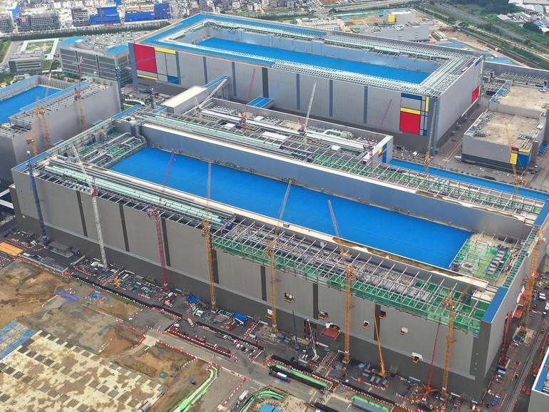
Samsung Electronics Co has started mass producing its latest dynamic random-access (DRAM) chip designed for mobile devices at its second semiconductor fabrication plant in Pyeongtaek.
The 16-gigabit Low Power Double Data Rate mobile DRAM uses extreme ultraviolet (EUV) technology.
According to Samsung, the EUV manufacturing process results in chips that are 30 percent thinner but faster, with data transfer rates of 6,400 megabits per second.
That means it can send 51.2GB of data per second.
According to Samsung, Pyeongtaek Line 2 is the world's largest semiconductor production line, as its total floor area spans more than 128,900 square meters, equivalent to about 16 football fields.
Samsung plans to spend over 30 trillion won on its second fab in Pyeongtaek, which will also have a foundry fabrication line and a NAND flash manufacturing facility.
Both facilities are expected to be fully operational in the second half of 2021.
Samsung is the leader of the global DRAM market.
It’s an important market for South Korean tech giant since the memory chip business accounts for about two-thirds of its revenue.


