


 Kingboard Holdings Shares Surge After HK$11.77 Billion Block Trade to Expand PCB and AI Supply Chain Business
  Trump Says Anthropic No Longer Seen as National Security Threat
  SoftBank Shares Drop as OpenAI Losses and Rising Costs Spark Investor Concerns
  Elon Musk Becomes World's First Trillionaire After SpaceX IPO Surge
  SpaceX Stock Gets $175 Target as Analysts See Massive Growth Ahead
  Meta AI Strategy Faces Challenges as Zuckerberg Admits Mistakes in Internal Memo
  Saudi Aramco Explores Sulphur Business Stake Sale to Raise Billions
  Chinese Social Media Giant Xiaohongshu Eyes Hong Kong IPO at Over $70 Billion Valuation
  Carro Expands Into Australia With Acquisition of Used-Car Platform CarPlace
  Obayashi to Acquire Multiplex in $526M Expansion Deal
  BHP Shares Fall as Jansen Potash Project Costs Surge
  US Raises Concerns Over Possible ASML EUV Machine Transfer to China
  Anthropic Officials Meet White House Over AI Model Outage
  GM and Lockheed Martin Partner to Strengthen U.S. Defense Manufacturing Capacity
  SK Hynix Shares Hit Record High After Shipping Next-Generation HBM4E AI Memory Samples
  Qantas Unveils Wellness-Focused Nonstop Sydney-London Flights to Reduce Jet Lag


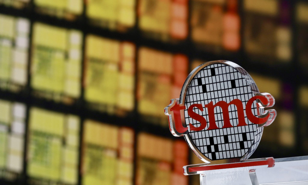
The computing chips driving artificial intelligence demand immense amounts of electricity, posing a growing challenge for data centers worldwide. On Wednesday, Taiwan Semiconductor Manufacturing Co. (TSMC), the world’s largest chip manufacturer and primary fabricator for Nvidia, revealed a groundbreaking strategy to improve chip energy efficiency by nearly tenfold—using AI-powered software to design them.
Today’s top AI servers, such as those running Nvidia’s flagship chips, can consume up to 1,200 watts during heavy workloads. Scaled across thousands of units, that level of energy draw is equivalent to powering 1,000 U.S. homes continuously. To combat this, TSMC is turning to advanced design methods and cutting-edge software tools developed in collaboration with Cadence Design Systems and Synopsys.
A key innovation lies in packaging multiple “chiplets”—smaller computing units made with different technologies—into a single system, creating far more efficient chip architectures. However, managing the complexity of such designs requires next-generation software. AI-driven design platforms are proving faster and more effective than human engineers for certain tasks, enabling chipmakers to unlock the full potential of TSMC’s 3D integration technology.
Jim Chang, deputy director of TSMC’s 3DIC Methodology Group, emphasized that AI tools are already outperforming engineers in some areas. “This thing runs five minutes while our designer needs to work for two days,” he explained, highlighting the speed and optimization advantages AI brings to chip development.
Yet, challenges remain. Moving data between chips using traditional electrical connections is hitting physical limits. Experts like Kaushik Veeraraghavan from Meta stress that optical connections may become the future for large-scale AI data centers. These advances will be critical as the world seeks more sustainable solutions to power the accelerating demand for AI computing.
By combining AI-driven design with innovative chip architectures, TSMC and its partners aim to set new standards for efficiency, performance, and scalability in the semiconductor industry.


